2D-PRINTABLE project
About 2D-PRINTABLE
2D materials have revolutionized the world of materials science and nanoscience. Thanks to their multitude of exceptional physical and chemical properties, they have enabled ground-breaking applications in various fields, such as optoelectronics, energy, sensing technology, and composite materials. However, the key to unlocking their full technological potential lies in finding cost-effective methods to harness these properties on a larger scale, to transfer the superlative electronic properties of individual nanosheets on macroscale samples. The 2D-PRINTABLE project is dedicated to achieving this goal by employing sustainable and affordable techniques known as liquid exfoliation methods. Through the 2D-PRINTABLE project, we will demonstrate that 2D materials are an indispensable asset in the field of printed electronics and have the potential to contribute significantly to addressing some of the world’s most pressing global challenges. The knowledge and innovations developed in this project will be instrumental for future emerging technologies in areas such as energy storage, water purification, environmental monitoring, as well as healthcare. Novel 2D materials can push the boundaries of current technology and provide a platform for the next generation of printed digital applications.
Objectives
To combine theoretical modelling, crystal growth and large-scale liquid-exfoliation, to scalably produce >20 new 2D Materials (2DMs) including conducting, semiconducting and insulating nanosheets with previously inaccessible aspect ratios.
To use chemical modification to further tune and optimize nanosheet properties (leading to >15 further variants) and provide a basis for functionalization and cross-linking as well as generating flake-level heterostructures of chemically bonded face-to-face combinations of different nanosheets.
To develop methods for large-scale (>10 cm2) liquid phase deposition of nanosheet networks including layer-by-layer assembly of nm-thick 2DMs into ordered multilayers.
To optimize these printed networks and heterostructures for digital systems, achieving new properties and functionalities.
To solution-deposit heterostructures using >20 combinations of both new 2DMs and the most promising existing ones in their pristine or functionalized form, optimize these printed networks and heterostructures for digital systems.
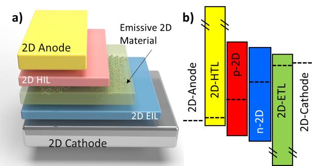
To demonstrate various printed digital devices including proof-of-principle, first time demonstration of all-printed, all-nanosheet, heterostack light-emitting diodes (LEDs).
Concept
The 2D-PRINTABLE project aims to integrate sustainable large-scale liquid exfoliation techniques with theoretical modelling to efficiently produce a wide range of new 2D materials (2DMs), including conducting, semiconducting, and insulating nanosheets. The focus includes developing the printing and liquid phase deposition methods required to fabricate networks and multicomponent heterostructures, featuring layer-by-layer assembly of nanometer-thick 2DMs into ordered multilayers. The goal is to optimize these printed networks and heterostructures for digital systems, unlocking new properties and functionalities. The project also seeks to demonstrate various printed digital devices, including proof-of-principle, first-time demonstration of all-printed, all-nanosheet, heterostack light-emitting diodes (LEDs). In conclusion, 2D-PRINTABLE will prove 2D materials to be an indispensable material class in the field of printed electronics, capable of producing far-beyond-state-of-the-art devices that can act as a platform for the next generation of printed digital applications.
Mission
2D-PRINTABLE joins a multi-disciplinary consortium with 7 Universities and 2 SMEs, located in 7 European countries including Italy, Germany, France, Ireland, United Kingdom, Estonia, and the Netherlands, to advance the field of 2D materials and unlock the full technology’s potential to play a significant role in the future of European digital electronics manufacturing.
This project will develop all-printed, all-nanosheet devices platform technology that could be used in a host of specific applications within the field of printed electronics. For example, such super-high-performance printed transistors will likely be combined in integrated circuits of increasing complexity for a range of applications such as low-cost/high-performance driver circuitry in applications such as active matrix displays (e.g., in smartphones) or wearable health monitoring devices (e.g., blood pressure or heart rate monitors).
2D-PRINTABLE Work Plan
Phase 1 – Designing and synthesizing novel 2D materials involves computational screening and literature analysis, focusing on substitutionally doped variants. These materials, including doped versions, are exfoliated in liquid media for use in printed digital devices. The outcomes are then passed on to the chemical modification stage, where nanosheets are altered to study their optical and physical properties, ultimately forming heterostructures with well-defined interfaces.
Phase 2 – The next phase concentrates on developing methods for printing or solution-depositing high-mobility networks of nanosheets, including flake-level heterostructures, while controlling interfaces. Subsequently, the characterization process comes into play, involving the comprehensive assessment of exfoliated and functionalized nanosheets, as well as the printed nanosheet networks and heterostructures, utilizing various spectroscopic and microscopic techniques.
Phase 3 – The electrical properties of individual flakes, networks, films, and heterostructures are then fully characterized to optimize their performance. This step establishes an understanding of charge transport, charge injection mechanisms, and structure-property relationships in printed structures.
Demo – Finally, the proof-of-concept stage demonstrates the potential of these novel 2D materials in traditional printed electronic devices, showcasing their application in high-performance thin-film transistors, demonstrator solar cells, and LEDs.
Results
Materials: >45 distinct innovative 2DMs: new unreported 2DMs; modified variants of known materials, materials previously unexfoliated, chemically modified/functionalised. New 2DMs available as printable inks, powders & films.
Networks & Heterostructures: New fabrication protocols for innovative printing & solution processing methods.
Breakthrough Devices: 1st all-printed, all nano-sheet LEDs, solar cells, high-performance transistors & memory elements + New fabrication protocols & full performance data.
Novel Characterization Methods: to demonstrate new properties/complementary functionalities of materials, networks, heterostructures, & devices.
Facts and figures
Acronym: 2D-PRINTABLE
Duration: 36 months
Start date: 1st October 2023
Total budget: 4,092,496.25€
EU Funding: 3,999,996.00€
Publications
2D-PRINTABLE is conducting research in the field of 2D materials and will disseminate scientific results to peers in the field through scientific publications. All relevant publications will be posted on this website.
Graphene Flagship
2D-PRINTABLE is part of the Graphene Flagship Initiative, specifically aligned within the “2D materials of tomorrow” focus area.
The Graphene Flagship Initiative, funded by the European Commission’s Horizon Europe research and innovation programme, represents 12 research and innovation projects and 1 coordination and support action with the collective mission to advance Europe’s strategic autonomy in technologies that rely on graphene and other 2D materials. To learn more visit: https://graphene-flagship.eu/