To fully harness the potential of 2D materials, it is crucial to optimize solution-deposition techniques for the fabrication of high-quality networks over large areas. These printed networks must exhibit properties suitable for device integration, such as high mobility and conductivity. A significant challenge in printing inks containing nanosheets with low aspect ratios is that such networks tend to be highly porous and disordered. As a result, the junctions between nanosheets, which are a key factor limiting the mobility and conductivity of the network, often form point-like structures with exceptionally high junction resistances.
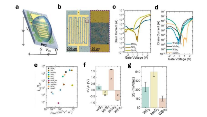
The developed transition metal dichalcogenides (TMDs) were successfully integrated into flexible devices. Optimization of all interfaces and components to maximize charge injection and transport was achieved by employing the Langmuir–Schaefer technique as the deposition process. The fabricated high-quality networks of nanosheets were embedded in TFTs exhibiting peak mobilities and on/off ratios of 101 cm2V -1s -1 and 105, respectively.
Read the full report on our website.