We are thrilled to announce that the second milestone of 2D-PRINTABLE: “Synthesis of first new layered crystals” has been completed.”
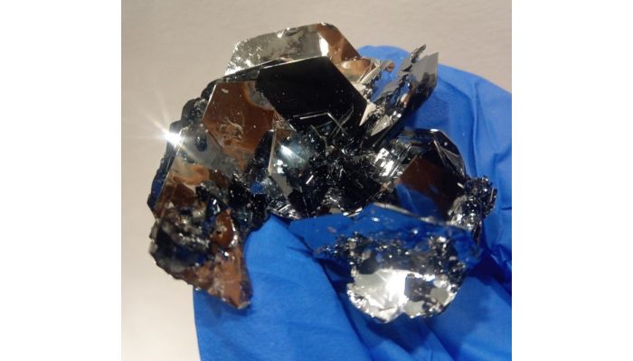
The basic set of 2D materials was developed and the procedures for their synthesis were standardized and scaled to at least 10 g per batch (in the research group of Prof. Sofer, UCT Prague). The large-scale growth was performed for several insulating materials including a 100 mm in diameter polycrystalline hBN bowl of thickness up to 1 mm with high breakdown voltage and lanthanum oxo-chloride as a representative of the high-k dielectric. For the semiconducting materials the growth was upscaled to 100 g for single crystals of molybdenum, tungsten diselenide, ditelluride and to 50 g for several other compounds including transition metal thiophosphites. From the group of metallic 2D materials the upscaled growth was performed for niobium and tantalum dichalcogenides up to 50 g batches and also optimized synthesis of MAX bulk phases was conducted and their exfoliation down to monolayer limit in gram scale for most common MXene compounds including Ti3C2Tx, Ti2CTx, V2CTx and others.
Various new 2D materials were developed including insulators, semiconductors and metals. High-k dielectric insulators were developed including lanthanum oxo-iodide and lanthanum oxo-bromide. From the semiconductor group several mixed thiophosphites such as CuScP2S6 and AgScP2S6 were synthesized as well as solid solutions like FeCoP2S6 and MnNiP2S6. From the group of metallic 2D materials a series of trichalcogenides like TaSe3 and mixed chalcogen of platinum like PdPtSe4 and PdSeTe were prepared.


