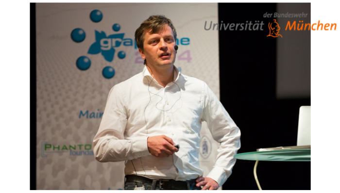
Georg S. Duesberg graduated in Physical Chemistry from the University of Kassel, Germany in 1996. After he was researcher at Max-Planck-Institute for Solid State Research, Stuttgart (MPI-FKF), Germany and Trinity College Dublin, Ireland from 1997–2001. He gained his PhD at the University of Tübingen, Germany in 2000.
From 2001–2007 he worked at the Infineon AG, Corporate Research Munich, and the Thin Films Department of Qimonda AG, Dresden on carbon hybrid devices. In 2007 Georg S. Duesberg became Principal Investigator at the Irish National Research Institute CRANN and Professor in the School of Chemistry of Trinity College Dublin, Ireland. Since 2017 Prof. Duesberg has a Chair for Sensortechnologies at the Institute of Physics and is spokesman of the Centre for Integrated Sensors (SENS) at the University of the Bundeswehr Munich.
His research covers the synthesis, characterization and devices fabrication of low-dimensional structures. He has worked on the fabrication of nanocarbon-silicon hybrid devices such as transistors, DRAMs, diodes, sensors and NEMS. Recently his research focuses on 2D Transitionsmetaldichalcogenides (TMDs), in particular PtSe2. Georg S. Duesberg has co-authored more than 300 publications with more than 50000 citations and has filed 25 patents.
What was your original motivation to become a researcher?
From my childhood on I loved to do experiments and explore. But there was not a clear plan. After my PhD, I worked in industry for seven years. But then I decided to get back into academia.
What is your (main) research area today?
Novel electronic materials and devices. To produce hybrid electronic devices by combining the opportunities of new materials and the power of silicon manufacturing is one of my favorite topics. For example, we fabricate nano-mechanical devices (NEMS) from TMDs, such as Platinumdiselinide (PtSe2), or graphene based bio-sensors in my labs.
What is the main objective of your team in 2D-PRINTABLE?
In the 2D-PRINTABLE we mainly deal with electrical characterization of 2D material films. For this we need to contact the materials with small electrical leads. In addition, we use sophisticated optical methods to deduce the electrical properties of 2D-based films.
What expertise and facilities does your team have to meet those objectives?
We have a large suit of electrical and optical methods to probe the electronic properties of thin films. We use e-beam lithography to structure and contact materials to create innovative devices. We have a set-up to do ThZ measurements at low temperatures on our films. We also have a tool to do LEIPS measurement that allows us – in combination with UPS – to derive the band gaps of thin films contactless.
Which aspects of your research at 2D-PRINTABLE do you believe are the most innovative and what unique opportunities offer 2D-PRINTABLE to yourself and/or your organisation?
The capability to be able to synthesis 2D materials and fabricated hybrid devices with them. In particular, we have sophisticated tools to probe and characterize ultrathin films.
How do you see the future use of the 2D-PRINTABLE results and the impact of 2D-PRINTABLE project in our daily lives?
Printable devices may have a huge impact on the fabrication of flexible and mobile opto-electronics devices